

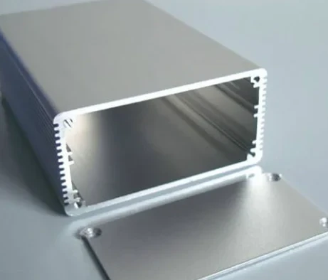
The transition to 5G infrastructure has changed the requirements for metal stamping processes. Operating in the millimeter-wave band above 24 GHz, signal behavior in this band is governed by the laws of physics and allows for no compromise. At these frequencies, even the slightest deviation in component geometry can directly result in measurable signal loss, impedance mismatch, and failure in compliance testing.
For 5G base stations, backplane connectors, and RF front-end module components, the manufacturing process is just as critical as the design itself. Metal stamping—particularly high-speed progressive die stamping—has become the preferred manufacturing process for connector terminals, contact pins, and EMI/RFI shielding housings. When executed properly, precision metal stamping can meet the micron-level tolerances, material consistency, and mass production requirements necessary for 5G deployment.
This article explores the application of custom metal stamping in the electronics and telecommunications industries, including technical requirements, material considerations, and process control.
The Challenges of 5G: Why Traditional Metal Stamping Processes Fall Short
Traditional metal stamping lacks the dynamic precision and feed accuracy required for 5G, as millimeter-wave frequencies demand dimensional stability within ±0.01 millimeters—far exceeding the ±0.1-millimeter tolerance range of traditional high-volume production equipment.
Dimensional Tolerances at Millimeter-Wave Frequencies
For consumer electronics, such as brackets or automotive structural components, standard metal stamping processes with tolerances within ±0.1 mm may still be acceptable. However, for 5G applications, such tolerances are far from sufficient.
Shielding enclosures and housings require tolerances of ±0.01–0.02 mm to form a seamless Faraday cage. Even a gap as small as 3 micrometers at a shielding seam can act as a slot antenna, radiating millimeter-wave energy and thereby reducing electromagnetic interference (EMI) shielding effectiveness. Connector housings and waveguides typically require a tolerance of ±0.05 millimeters to maintain RF signal integrity and proper mating alignment. Terminals and contacts—the components that actually carry the signal—require tolerances as tight as ±0.003 mm to prevent intermittent connections and poor contact.
There is virtually zero margin for error. If a metal stamping manufacturer fails to detect a 0.03 mm tolerance drift, it could render an entire batch of connector housings unusable.
Electromagnetic Interference (EMI) Shielding Performance Requirements
Shielding performance is measured in decibels (dB) of attenuation. For 5G applications at millimeter-wave frequencies, the target attenuation is typically 40–60 dB. This level of shielding cannot be achieved if seam gaps are poorly finished, wall thickness is uneven, or edges have burrs, leading to a failure of the electromagnetic seal.
Traditional metal stamping for shielded enclosures often fails when working with high-strength cold-rolled steel or stainless steel. Material springback can cause forming angles to exceed tolerance limits. The accumulation of minute tolerances between stations in a progressive die reduces the final coplanarity, leading to surface-mount technology (SMT) soldering defects—such as cold solder joints or solder bridges—which compromise SMT yield.
A shielding enclosure is not simply a box. It is a precision electromagnetic structure, and the custom metal stamping process must be engineered accordingly.
Key Components of 5G Metal Stamping
Key components in the 5G metal stamping process—connector terminals and electromagnetic interference (EMI) shielding layers—require micron-level precision and controlled material properties to maintain signal integrity and achieve 40–60 dB attenuation at millimeter-wave frequencies.
Connector Terminals and Contact Pins
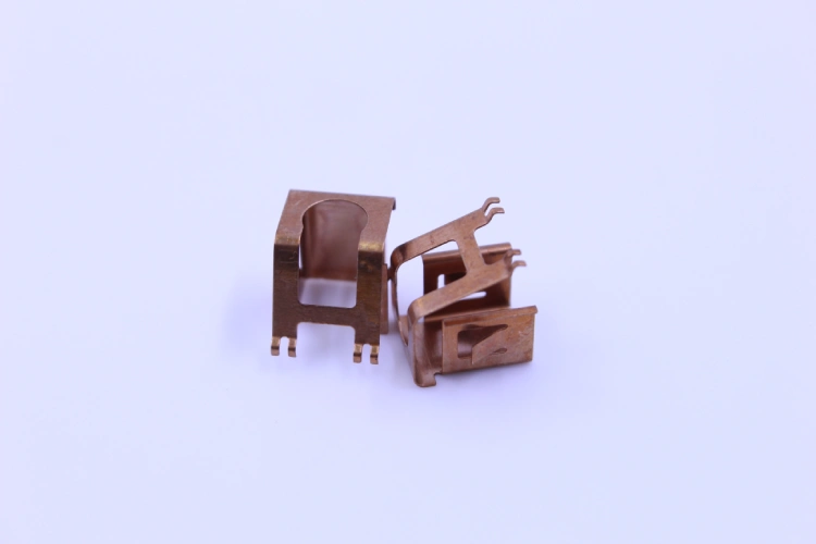
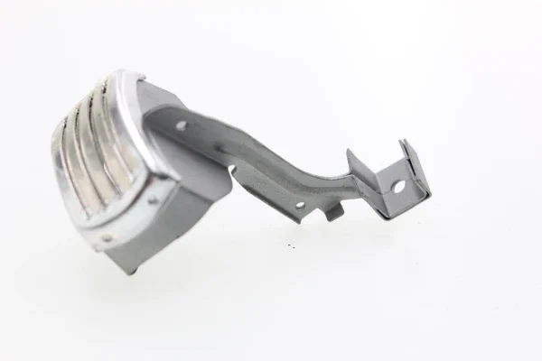
Connector terminals are critical components for signal transmission in any 5G system. They must maintain constant contact pressure, low and stable resistance, and geometric integrity throughout millions of mating cycles.
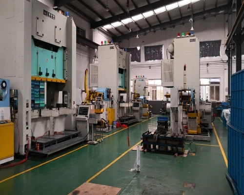
Connector terminals are typically manufactured using progressive metal stamping, which sequentially performs multiple processes: blanking, punching, forming, bending, coining, and trimming. High-speed stamping presses operating at 800 to 1,200 strokes per minute can produce these components at a throughput unmatched by machining or additive manufacturing.
The material of choice for high-performance terminals is beryllium copper, specifically the C17200 alloy. This alloy exhibits exceptional electrical conductivity, elastic limit, and fatigue resistance, with overall performance comparable to that of specialized steels.
However, beryllium copper presents a long-standing challenge: springback. The material’s high elastic limit means it tends to return to its original shape after forming. To successfully perform custom metal stamping of beryllium copper terminals, springback compensation mechanisms must be incorporated into the die design, and careful consideration must be given to grain orientation, bend radius, and carrier strip layout.
EMI/RFI Shielding Enclosures and Chassis
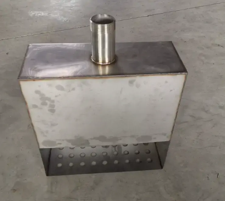
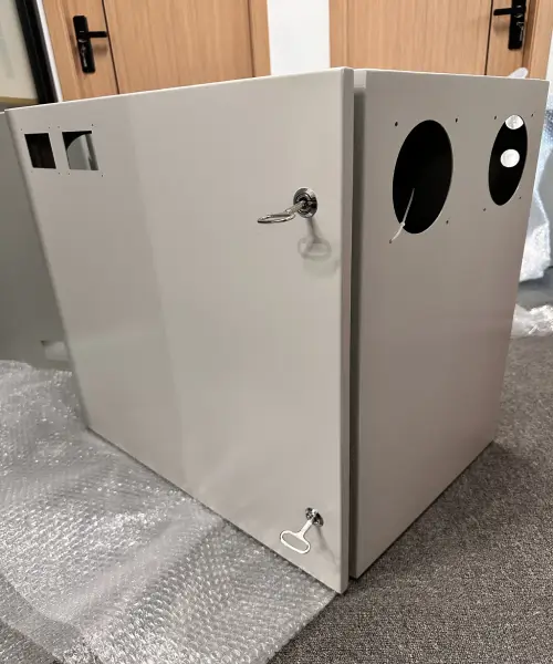
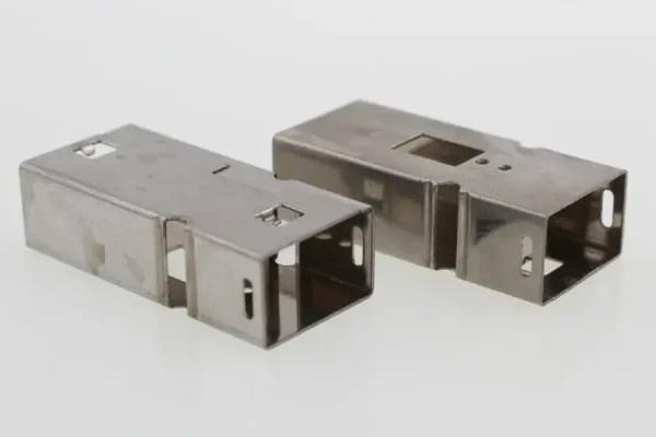
Electromagnetic interference (EMI) shielding enclosures serve a dual purpose: they contain electromagnetic radiation generated by the shielded components while protecting them from external interference. For 5G equipment, these enclosures must also provide effective heat dissipation and be compatible with automated surface-mount technology (SMT) processes.
Shielding enclosures are typically made from thin-gauge materials—often less than 0.2 millimeters thick. Nickel-silver alloys offer excellent weldability and electrical conductivity. Stainless steel provides corrosion resistance and rigidity for outdoor enclosures. Aluminum combines a lightweight structure with good electrical conductivity.
Producing deep-drawn EMI shielding enclosures (i.e., the currently dominant seamless, one-piece design) using the metal stamping process presents significant mechanical challenges. Ultra-thin materials are extremely sensitive to drawing stress. Even slight tension fluctuations at the decoiler or micron-level pitch errors during feeding can cause wrinkling, tearing, or uneven wall thickness during the deep-draw metal stamping stage.
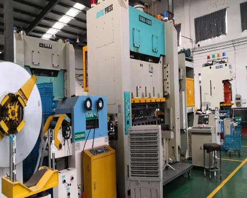
Advanced precision metal stamping production lines address this issue by using horizontal decoilers to eliminate gravity sagging and employing zero-tension feeding to preserve the material’s grain structure.
Only 4 steps
online custom metal fabrication parts
Contact our experts team and experience the efficiency and economic benefits of digital metal fabrication services.
Upload Design Files
STL , STEP (.stp), IGES (.igs), (.ZIP), or PDF.
Also be a sample or an idea
Quote & Design Analysis
Instant factory quotes and DfM reports, the most reasonable solution.
Manufacturing Begins
Digital processes can initiate order tasks within 24 hours.
On-Time Delivery
Keeping delivery promises, approved by 3000+ Global Company buyers.
Material Selection for 5G Metal Stamping Applications
The choice of materials for custom metal stamping directly determines formability, die life, and the performance of the final components—copper alloys are used to enhance electrical conductivity, stainless steel is used for shielding, and thickness tolerances determine process stability.
Copper Alloys: Beryllium Copper and Phosphor Bronze
Beryllium copper—specifically C17200—is the benchmark material for 5G connector terminals. Its composition provides both high electrical conductivity and fatigue resistance comparable to that of special steels. The challenge with C17200 in precision metal stamping lies in its elastic limit; the material experiences significant springback after forming. To successfully perform progressive metal stamping, it is essential to integrate a bend compensation mechanism into the die, control the grain orientation so that it aligns with the bending axis, and employ a carrier strip design that minimizes stress concentration.
For less demanding applications, phosphor bronze is a lower-cost alternative. It offers sufficient elasticity but has lower electrical conductivity and fatigue life. For procurement teams, the key decision factor is cycle life—beryllium copper terminals can withstand over 10,000 insertion and removal cycles, while phosphor bronze typically has an upper limit of fewer than 5,000 cycles.
Material certification must verify the alloy composition and temper, as even minor deviations can affect springback behavior and final contact pressure.
Stainless Steel and Nickel-Silver Alloys
For 5G shielded enclosures requiring corrosion resistance or structural rigidity in outdoor installations, stainless steel (typically 301 or 304) is usually specified. Stainless steel stamping presents a range of distinct challenges. Its high work-hardening rate accelerates die wear. Without coated dies and proper lubrication, edge quality deteriorates rapidly.
For shielded enclosures that must withstand SMT reflow soldering temperatures (typically peaking at 260°C), nickel silver alloys (copper-nickel-zinc) are commonly selected. The nickel content ensures solderability and oxidation resistance. Both materials require slower feed rates, higher forming pressures, and frequent maintenance of metal stamping dies.
Special attention must be paid to the surface finish of the material. Surface roughness affects both electromagnetic interference (EMI) attenuation and solder wettability.
Metal Stamping Material Thickness and Tolerances
Sheet metal thickness in 5G precision metal stamping typically ranges from 0.1 mm to 0.4 mm, with many components tending toward the lower end of this range. At these thicknesses, conventional dies cannot produce burr-free edges—micro-stamping or fine blanking becomes essential.
The thickness tolerance of the incoming steel strip is equally critical. Steel mills typically supply material with a tolerance of ±0.01 millimeters, but this tolerance alone is sufficient to cause dimensional deviations in the final part. In progressive die metal stamping with multiple forming stations, a 0.005-millimeter difference in thickness at the blanking station can result in measurable springback deviations at the final forming station.
Therefore, incoming inspection procedures are critical. If a custom metal stamping shop does not verify the thickness of each coil of strip steel and reject material that falls outside the tolerance range upon arrival, it will be unable to produce dimensionally consistent parts, no matter how advanced the metal stamping production line may be.
High-Speed Precision Metal Stamping Process Engineering
To achieve micron-level tolerances in high-speed metal stamping, synchronized control of die design, vibration damping, feed accuracy, and process validation is essential—these are indispensable prerequisites, not optional considerations.
Progressive Die Design and Metal Stamping Die Manufacturing
The design of a progressive die directly determines whether the metal stamping process can maintain a tolerance of ±0.01 millimeters over 500,000 stamping cycles. The choice of die steel—powder metallurgy grades or tungsten carbide inserts—enables the die to withstand abrasive wear and maintain sharp cutting edges during high-speed cycles. TiAlN-coated punches reduce friction and heat generation, extending die life during production by 300%.
Each forming station incorporates a springback compensation design that corrects elastic springback via over-bend angles and coining blocks before the workpiece exits the die. The strip layout must balance material utilization with geometric stability to prevent deformation caused by uneven stress distribution. Without these design elements, progressive die metal stamping cannot meet the consistency requirements of 5G.
A manufacturer’s in-house die-making capability is a key differentiator in the field of high-speed metal stamping—outsourced dies rarely achieve the required Cpk targets.
Vibration Control and Dynamic Accuracy in Metal Stamping
Destructive vibrations generated by high-speed presses operating at 800 to 1,200 strokes per minute can degrade the quality of precision metal stamping parts and accelerate die wear. A rigid frame structure equipped with a precision guidance system maintains punch parallelism and absorbs kinetic energy during the stamping process. Vibration-damping materials integrated into the press bed reduce harmonic resonance, which would otherwise cause deviations in forming angles.
Dynamic precision also depends on the press’s drive system—direct-drive servo presses offer better speed control performance compared to traditional flywheel designs. The cumulative effect of micrometer-level vibrations manifests as fluctuations in burr height and inconsistent bend radii. Custom metal stamping production lines without active vibration monitoring cannot meet the tolerance requirements for 5G connectors. In the metal stamping process, the specifications of the press are just as important as the die design—while older presses may have good mechanical performance, they lack the dynamic stiffness required to produce millimeter-wave components.
Feeding Accuracy and Synchronization
Feeding accuracy is the foundation of dimensional consistency in progressive metal stamping. Mechanical roller feeders driven directly by the press’s eccentric shaft can achieve micron-level pitch accuracy and eliminate the electronic delays inherent in servo systems.
For high-strength materials such as stainless steel, closed-loop CNC servo feeders have replaced mechanical drive systems, enabling fine adjustments at every step. Synchronization between the feeder and the press is critical—a pitch error of 0.02 millimeters at the first station will be continuously amplified in subsequent forming stations, leading to cumulative drift and compromising coplanarity.
Advanced metal stamping production lines employ cam-driven feeding systems to ensure that the strip is properly positioned within the die cavity before the punch is lowered. Since thickness variations affect feeding grip, the feed roller pressure and strip straightening parameters must be calibrated individually for each coil of steel.
Quality Control in the Precision Metal Stamping Production Process
Quality control during production is a minimum requirement for 5G high-speed metal stamping. Real-time tonnage monitoring detects punch wear or changes in material hardness before defects occur. Sensors inside the die verify part dimensions at critical process points, triggering an automatic shutdown when readings exceed control limits. An automatic optical inspection (AOI) system provides 100% dimensional verification at production speeds, with measurement accuracy for critical features reaching ±0.005 millimeters.
Statistical Process Control (SPC) tracks the Capability Index (Cpk) for each critical feature; when Cpk falls below 1.67, the system triggers corrective actions. Without these control measures, compliant parts and scrap from the metal stamping production line would be mixed together, and downstream assembly processes would be unable to detect this. A metal stamping manufacturer’s investment in measurement equipment and real-time data systems demonstrates its genuine commitment to quality—rather than relying solely on sorting at the end of the production line.
Quality Standards and Requirements for Metal Stamping Manufacturers
Quality standards for 5G precision metal stamping extend beyond part dimensions—IATF 16949 certification and material traceability verify process compliance and supply chain integrity from coil stock to finished components.
IATF 16949 and PPAP Requirements
IATF 16949 certification demonstrates that a metal stamping manufacturer operates under a quality management system established to achieve zero-defect production. For 5G components, the standard’s mandatory elements—control plans, PFMEA, measurement system analysis (MSA) including gage repeatability and reproducibility (Gage R&R), and statistical process control—are directly applicable to the quality requirements of the telecommunications industry.
Tier-1 OEMs are increasingly requiring the submission of Level 3 PPAP documentation. This documentation package is used to verify that manufacturers can consistently maintain the dimensional accuracy of precision metal stamping parts prior to mass production. Key components include dimensional measurement results, material test reports, capability studies (Cpk ≥ 1.67), and measurement system analysis.
For procurement departments, PPAP is not merely paperwork—it is critical evidence. Manufacturers unable to submit a complete Level 3 PPAP documentation package lack the process discipline required for 5G high-speed metal stamping. Without these controls, tolerance drift will go unnoticed until it is discovered upon receipt of customer returns.
Material Traceability and Surface Treatment
Traceability in custom metal stamping begins with the steel mill certificate—which includes alloy composition, condition, thickness tolerances, and furnace lot number. Each coil of steel must be registered against the production order, and every metal stamping batch must be traceable to that specific coil. The performance of beryllium copper depends on precise chemical composition; a deviation of just 0.1% in beryllium content can alter springback and electrical conductivity.
Surface treatment is equally critical. Coining stations within the metal stamping die can polish edges to a surface roughness of Ra 0.4 micrometers, eliminating micro-burrs prior to plating. For electromagnetic interference (EMI) shielding components, surface roughness directly affects attenuation—rough surfaces create air gaps that weaken the shielding effect. For connectors, contaminated surfaces can lead to failure of plating adhesion.
The procurement department must verify that the metal stamping manufacturer performs incoming inspections on every coil of material and maintains lot-level traceability throughout the entire stamping production line. Otherwise, if material mix-ups occur, they cannot be effectively controlled.
Conclusion
High-speed precision metal stamping for 5G connectors and electromagnetic interference (EMI) shielding housings is not a typical metalworking service. It requires adherence to rigorous engineering standards at every stage—from material selection and die design to vibration control and process validation.
A tolerance deviation of just 0.03 millimeters can result in the entire production batch being scrapped; a 3-micrometer gap in the shielding seam can turn an EMI shield into a slot antenna; and a 0.5-micrometer deviation in high-frequency terminals can lead to a 15% loss in signal capacity.
For procurement professionals, the path to ensuring a reliable supply is clear: specify GD&T annotations for critical dimensions, require a Cpk value of ≥1.67 for critical features, adopt a progressive die metal stamping process equipped with statistical process control (SPC), and validate production capability through PPAP before mass production begins.
Supro is a precision metal stamping manufacturer based in China. We operate a 2,500-square-meter precision stamping facility equipped with 80 sets of press machines ranging from 6 metric tons to 1,000 metric tons, capable of processing materials with thicknesses from 0.005 inches to 5 inches and manufacturing stamped parts up to 24 inches in width. Supro ships over 5 million precision metal stamping parts annually to customers worldwide and maintains an annual production capacity of 1,000 metric tons. If you need custom metal stamping services, please contact us today!