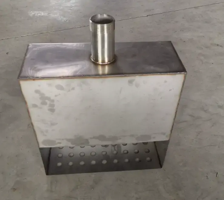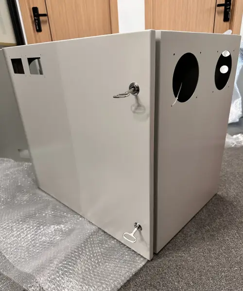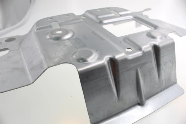

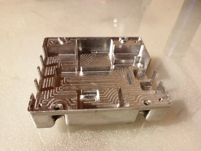
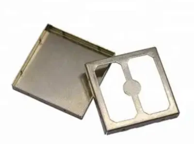
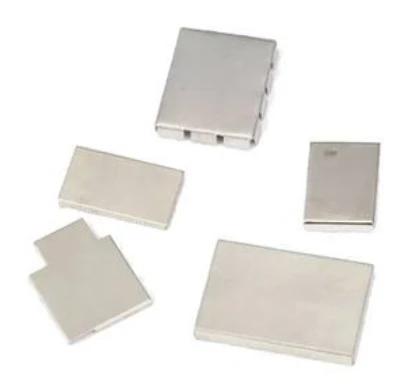
EMI shielding cans—also known as radio frequency (RF) shielding cans or board-level shielding cans—are metal enclosures mounted over sensitive components or sections of a circuit to block EMI/RFI radiation and prevent external interference. In a wide range of applications, from wireless communications and medical devices to automotive electronics, these components are essential for achieving electromagnetic compatibility (EMC) compliance.
However, a problem arises when implementing EMI shielding cans: the shielding, which is intended to protect the circuit, can under certain conditions actually become the root cause of catastrophic hardware failure. When the inner top surface of an EMI shielding can comes into contact with exposed pins or active components on a printed circuit board (PCB), it causes a direct short circuit—which typically results in permanent damage to the board and its components.
From the perspective of precision metal fabrication, this failure mode in EMI shielding cans is entirely preventable. Its root causes—insufficient Z-axis height clearance, thermal deformation under operating conditions, and a lack of internal dielectric insulation—are well understood, and corresponding countermeasures are technically effective and suitable for mass production.
This article will explore this failure mechanism, its root causes, and manufacturing-level solutions capable of eliminating this risk.
Understanding the Risk of Short Circuits in EMI Shielding Cans
EMI shielding cans function similarly to a grounded Faraday cage. By enclosing sensitive components or circuit sections within them, they block radiated interference and prevent external interference. During normal operation, the shielding can is connected to the PCB ground plane via soldering, thereby establishing a low-impedance return path that diverts electromagnetic energy to ground. Its internal space must be large enough to accommodate the components to be shielded without coming into physical contact with them.
Failures occur when this gap is compromised. The inner surface of the top of the EMI shielding can—typically made of tin-plated steel, nickel silver, or a copper alloy—may come into unintended contact with components or exposed leads. Since the shielding can is grounded, this contact creates a direct short to ground, bypassing the component’s intended return path and often conducting fault currents directly into sensitive circuits. The consequences range from intermittent failures and system resets to permanent damage to components and surrounding circuits.
In high-reliability applications—such as medical devices, automotive electronics, and wireless infrastructure—such failures not only result in yield losses but also pose a field reliability risk that may evade standard electrical testing. Therefore, it is crucial to understand the physical conditions that trigger this failure mode in EMI shielding cans before implementing corrective measures at the manufacturing level.
Root Cause Analysis of Short Circuits in EMI Shielding Cans
Short circuits in EMI shielding cans may stem from the following three root causes: insufficient Z-axis height clearance to accommodate cumulative tolerances; thermal warping caused by mismatched coefficients of thermal expansion; and the absence of an internal insulation layer to isolate the grounded housing from component leads.
Insufficient Z-Axis Height Allowance in Custom EMI Shielding Cans
Insufficient Z-axis height allowance is the most direct cause of short circuits in EMI shielding cans. Manufacturing tolerances for standard sheet metal stampings typically fall within the range of ±0.1 mm to ±0.2 mm, while high-precision dies can achieve tolerances within ±0.05 mm. However, when cumulative tolerances on the PCB assembly side—including component placement deviations, solder paste thickness variations, and PCB warpage—are combined with the manufacturing tolerances of the EMI shielding can, the result often exceeds the nominal clearance value established during the design phase.
When the total cumulative tolerance exceeds the reserved Z-axis clearance, the inner top surface of the custom EMI shielding can comes into physical contact with the components or exposed leads below. Since the shielding can is soldered to the PCB’s ground plane, this contact directly creates a short circuit to ground.
If a comprehensive tolerance stack-up analysis is not performed during the design phase, and clearance planning relies solely on nominal dimensions rather than worst-case conditions, such risks are difficult to identify at the design stage.
Thermal Deformation Under Operating Conditions
Thermal deformation is a key factor causing the gap between EMI shielding cans to dynamically decrease during service. It is a fundamental physical law that metals expand when heated and contract when cooled. After an EMI shielding can is soldered to a PCB, there is a significant difference in the coefficients of thermal expansion (CTE) between the metal can (typical CTE of approximately 17 ppm/°C) and the PCB substrate (FR-4 has a CTE of approximately 14–16 ppm/°C, depending on the orientation of the glass fiber weave). This CTE mismatch generates thermal stress as the device’s operating temperature rises, causing the EMI shield can to warp locally or cave inward.
For stamped shield cans made from thin materials ranging from 0.12 mm to 0.3 mm, repeated thermal cycling is particularly detrimental. When thermal deformation causes micrometer-level displacement toward the inner top surface, the Z-axis clearance—which was already at a critical level—is breached, triggering intermittent or permanent short circuits. Furthermore, the preheating and cooling phases of the reflow soldering process inherently introduce residual stresses, which further exacerbate the tendency of custom EMI shielding cans to deform.
Lack of Internal Insulation in EMI Shielding Cans
The absence of an internal insulation layer means that short-circuit protection for EMI shielding cans relies entirely on a single line of defense: the mechanical gap. Most shielding can designs feature conductive metal inner surfaces that directly face the PCB components, with no dielectric barrier between the can and the components. When the Z-axis gap is reduced to zero due to cumulative tolerances or thermal deformation, there is no secondary protection mechanism to block the electrical path.
This design flaw is particularly dangerous in high-voltage applications—even if the gap has not completely disappeared, air breakdown (arcing) may still occur when the electric field strength exceeds the dielectric breakdown threshold of air, resulting in a short circuit equivalent to physical contact.
From a sheet metal fabrication perspective, the absence of an internal insulating layer is not a manufacturing error but a systemic defect resulting from an inadequate Failure Mode and Effects Analysis (FMEA) during the design phase of custom EMI shielding cans.
Integrating an insulating material lamination process into the stamping and forming process of EMI shielding cans is an effective way to address this design shortcoming from the manufacturing end.
Only 4 steps
online custom metal fabrication parts
Contact our experts team and experience the efficiency and economic benefits of digital metal fabrication services.
Upload Design Files
STL , STEP (.stp), IGES (.igs), (.ZIP), or PDF.
Also be a sample or an idea
Quote & Design Analysis
Instant factory quotes and DfM reports, the most reasonable solution.
Manufacturing Begins
Digital processes can initiate order tasks within 24 hours.
On-Time Delivery
Keeping delivery promises, approved by 3000+ Global Company buyers.
Preventive Strategies to Avoid Short Circuits in EMI Shielding Cans
To prevent short circuits in custom EMI shielding cans, a systematic approach is required: applying an internal dielectric insulation layer, conducting 3D interference checks that account for worst-case tolerance accumulation, and implementing design-for-manufacturing practices to control thermal deformation and material variability starting from the stamping process.
Kapton® Polyimide Insulation Material as the Primary Solution
Applying Kapton® polyimide tape to the inner surface of custom EMI shielding cans creates a robust dielectric barrier while adding only a minimal amount of thickness, thereby maintaining the critical Z-axis clearance.
Material Characteristics and Electrical Properties
Polyimide film combines excellent electrical, thermal, and mechanical properties, making it particularly suitable for insulating the interior of EMI shielding cans.
The film is yellow and transparent, with a density of approximately 1.42 g/cm³. It has a wide long-term operating temperature range, capable of sustained use from -269°C to 260°C, and can withstand short-term temperatures as high as 400°C. This not only meets the thermal requirements of reflow soldering but also withstands the high junction temperatures of power devices during normal operation.
Polyimide film possesses excellent electrical insulation properties, with a dielectric constant of approximately 3.4–4.0, a dielectric loss of 0.004–0.007, and a dielectric strength of 100–300 kV/mm, classifying it as an F- to H-class insulation material. It also exhibits excellent mechanical properties, with a tensile strength of up to 200 MPa and an elongation at break (longitudinal) of no less than 55%.
From the perspective of EMI shielding can manufacturing, its thin structure—typically with a film thickness of 0.025 mm to 0.05 mm—results in only minimal dimensional accumulation, thereby preserving rather than consuming critical Z-axis clearance.
For applications requiring a balance between cost and performance, Mylar (polyester) film is a viable alternative, as its dielectric properties are sufficient to meet the requirements of low-voltage environments.
Automation Applications in EMI Shielding Can Manufacturing
Integrating the Kapton® tape lamination process into the production workflow for custom EMI shielding cans requires striking a balance between precision, throughput, and cost through process design.
The tape is supplied in rolls and laminated using automated pick-and-place equipment equipped with precision die-cutting stations. Depending on the part geometry and production batch size, the application process can be scheduled either before or after the stamping and forming operations. For EMI shielding cans with simpler designs—that is, cans with flat tops and few deep-drawn features—pre-laminating the tape onto flat blanks prior to stamping achieves the highest throughput, as the tape is applied and die-cut in a continuous roll-to-roll process.
For EMI shielding cans with complex geometries—such as deep draws, ribs, or embossed features—using a robotic placement system to apply the tape after forming ensures precise positioning and complete coverage of the inner top surface, without wrinkles or curled edges.
Automated vision systems verify tape positioning and detect defects such as wrinkles, gaps, or misalignment—these critical quality checkpoints cannot be reliably achieved through manual application in mass production.
3D Interference Checks for EMI Shielding Cans During Design Verification
Conducting 3D interference checks on custom EMI shielding cans during the design verification phase—by accounting for worst-case component heights and cumulative manufacturing tolerances—ensures sufficient clearance in the Z-axis direction, thereby eliminating the risk of contact before finalizing the mold design.

CAD-Based Clearance Verification
CAD-based 3D interference analysis provides a virtual environment for evaluating the physical clearance between the inner surface of custom EMI shielding cans and the components they enclose. This analysis must account for the full stack-up of tolerances: PCB thickness variations (typically ±10%), component placement tolerances, solder paste deposit height, and the stamping dimensional tolerances of the shielding can itself.
Responsible EMI shield can design verification should not evaluate clearances based solely on nominal values but should employ a worst-case tolerance analysis—that is, aggregating the maximum material conditions for all relevant dimensions. If the cumulative tolerance exceeds the specified Z-axis clearance, interference is predicted to occur. Industry standards such as IPC-2221 provide guidance on minimum component clearances based on PCB categories and application requirements.
Furthermore, the analysis must account for thermal expansion: a mismatch in the coefficients of thermal expansion (CTE) between metal EMI shielding cans (approximately 17 ppm/°C for steel) and the PCB substrate (14–16 ppm/°C for FR-4) can lead to differential displacement as temperatures rise. A robust CAD verification process can flag clearance violations before steel cutting, allowing for design corrections at minimal cost.
Prototype Verification
Although CAD-based analysis can identify theoretical clearance risks, physical prototype verification is required to confirm whether the actual hardware behavior matches the model.
Prototype assemblies should be inspected via sectioning or X-ray inspection to directly measure the internal clearances between EMI shielding cans and the underlying components. X-ray imaging enables non-destructive visualization of Z-axis clearances, revealing localized clearance reduction that CAD models may fail to capture—such as variations in solder joint height, component coplanarity issues, or subtle shield deformation caused by stamping and forming processes.
For high-reliability applications, thermal cycling tests are critical: by monitoring the gaps while exposing the prototype to extreme operating temperature environments, these tests reveal dynamic gap narrowing that static measurements cannot detect.
The validation program should also include mechanical shock and vibration testing to ensure that the clearances in the EMI shield can are maintained under actual operating and transportation conditions. Prototype validation enables closed-loop verification between design intent and physical reality, allowing the detection of issues such as cumulative tolerances, material inconsistencies, and assembly deviations that go unnoticed in virtual analysis.
Manufacturing Design Considerations for EMI Shielding Cans
Addressing the risk of short circuits in custom EMI shielding cans during the design-for-manufacturing phase requires strategic material selection, structural features that maintain clearances under stress, and strict process control to ensure dimensional accuracy consistency throughout the production process.
Material Selection and Thickness
The choice of material for EMI shields directly affects shielding effectiveness at the target frequency as well as mechanical performance under thermal loads.
For applications above 15 MHz, shielding is primarily due to the skin effect—as long as the thickness is at least 0.05 millimeters (0.002 inches), almost any metal (including brass, nickel silver, copper, and steel) can provide adequate attenuation.
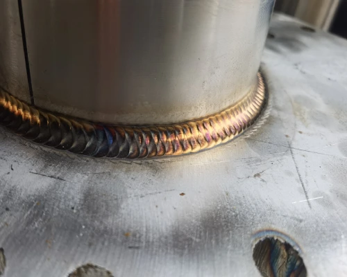
For shielding components requiring manual soldering or reflow soldering with flux, nickel silver (55% copper, 27% zinc, 18% nickel) is inherently solderable and does not require subsequent electroplating, thereby shortening lead times and reducing costs.
Thickness selection involves trade-offs: thicker gauges (0.20 mm to 0.50 mm) offer higher mechanical rigidity and resistance to thermal warping, while thinner gauges (0.10 mm to 0.15 mm), although they reduce material costs and weight, are more prone to deformation under thermal cycling conditions.
For high-reliability EMI shield can applications with stringent thermal requirements, selecting thicker gauges within this range—0.25 mm to 0.30 mm—provides significant margin against thermal warpage without compromising formability.
Structural Features for Clearance Management
Incorporating geometric features into the design of custom EMI shielding cans can provide additional Z-axis clearance for tall and short components without increasing the overall height of the can.
Embossed or dimpled features—that is, localized raised areas formed on the top surface of the can—can precisely provide additional clearance space at the locations of tall and short components. These features are created during the stamping process using specialized forming stations in progressive dies, significantly increasing clearance space at minimal additional cost.
Depressed areas formed on the top surface of EMI shielding cans through embossing or shallow drawing processes create spacer zones, thereby maintaining clearance above components such as connectors, tall and short capacitors, or power inductors.
Ventilation holes—appropriately sized slots or perforations—serve a dual purpose: they reduce internal operating temperatures by promoting airflow circulation, thereby minimizing thermal deformation; at the same time, when the aperture size is controlled to be less than one-twentieth of the relevant shortest wavelength, they also maintain shielding effectiveness.
In two-piece frame-and-cover designs, the frame provides structural rigidity and consistent spacing height, while the removable cover allows for inspection without compromising the dimensional stability of the shielding enclosure.
Tolerance Control in EMI Shielding Can Manufacturing
Tolerance control is the cornerstone of reliable EMI shielding can production. Standard stamping tolerances of ±0.1 millimeters can be achieved using conventional dies, while high-precision progressive dies can consistently achieve tolerances of ±0.05 millimeters or better. For the critical Z-axis clearance, the height dimension of the EMI shielding can must be controlled even more strictly.
Statistical Process Control (SPC) during production monitors critical dimensions in real time, issuing drift alerts before parts exceed specification limits. Die maintenance schedules must account for die wear, as dimensional deviations gradually increase with each production batch. Fluctuations in coil thickness—typically ranging from ±5% to ±10% of the nominal thickness—must be factored into the tolerance analysis.
Supro is a specialized manufacturer of EMI shielding cans. We validate our prototype molds using the same material batches and thicknesses as those used in mass production to ensure that gap verification results obtained from prototypes can be directly applied to mass-produced parts.
Looking for a reliable custom sheet metal fabrication companies?
Talk To Supro MFG Expert Team
Contact us for competitive ex-factory prices,
and a full range of technical support services.
Conclusion
Short-circuit issues in EMI shielding cans are a preventable failure mode caused by the combined effects of design assumptions, manufacturing tolerances, and thermophysical factors. From a precision metal fabrication perspective, the solution requires a multi-layered strategy:
Ensure sufficient clearance in the Z-axis direction to accommodate all tolerance accumulation and thermal expansion.
Incorporate an internal dielectric insulation layer (such as Kapton tape or equivalent material) as a secondary protective layer.
Conduct rigorous 3D interference checks during the design verification phase.
Implement controlled manufacturing processes to achieve consistent dimensional accuracy.
Supro is a professional manufacturer of EMI shielding cans with over 20 years of experience in custom sheet metal fabrication. Leveraging our advanced equipment, extensive manufacturing expertise, and professional engineering team, we provide perfect custom EMI shielding can solutions to more than 3,000 companies worldwide, along with genuine manufacturer quotes.
If you require engineering consultation or design-for-manufacturing support, please contact our technical team.